

'%3e%3cpath%20d='M12%2020.3333C16.6024%2020.3333%2020.3333%2016.6024%2020.3333%2012C20.3333%207.39762%2016.6024%203.66666%2012%203.66666C7.39763%203.66666%203.66667%207.39762%203.66667%2012C3.66667%2016.6024%207.39763%2020.3333%2012%2020.3333Z'%20stroke='%23F2F2F2'%20stroke-width='2.08333'%20stroke-linecap='round'%20stroke-linejoin='round'/%3e%3cpath%20d='M8.66667%2013.6667C8.66667%2013.6667%209.91667%2015.3333%2012%2015.3333C14.0833%2015.3333%2015.3333%2013.6667%2015.3333%2013.6667'%20stroke='%23F2F2F2'%20stroke-width='2.08333'%20stroke-linecap='round'%20stroke-linejoin='round'/%3e%3cpath%20d='M9.5%209.5H9.50833'%20stroke='%23F2F2F2'%20stroke-width='2.08333'%20stroke-linecap='round'%20stroke-linejoin='round'/%3e%3cpath%20d='M14.5%209.5H14.5083'%20stroke='%23F2F2F2'%20stroke-width='2.08333'%20stroke-linecap='round'%20stroke-linejoin='round'/%3e%3c/g%3e%3cdefs%3e%3cclipPath%20id='clip0_10282_1064'%3e%3crect%20width='20'%20height='20'%20fill='white'%20transform='translate(2%202)'/%3e%3c/clipPath%3e%3c/defs%3e%3c/svg%3e)


Electronic circuit diagram showing a ZVS-QRAS Marx stage.
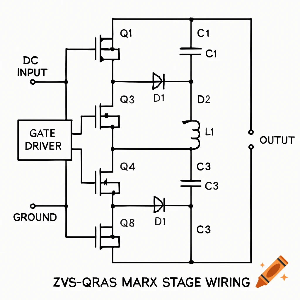
Here’s a comprehensive wiring guide for your 6-stage ZVS-QRAS Marx generator, including schematics, component placement, and critical layout details. This ensures optimal performance, safety, and efficiency. 1. Stage-by-Stage Wiring Diagram Each stage consists of 4x GaN FETs, 2x capacitors, 2x diodes, and LC snubbers. Below is the wiring for one stage (repeat ×6 for full Marx): Schematic ZVS-QRAS Marx Stage Wiring (Visual reference: Replace with actual schematic) Connections per Stage: Component Connection Points Notes GaN FETs (Q1-Q4) Q1/Q2: Source → Ground, Drain → Capacitor (+) Charging switches (parallel). Q3/Q4: Source → Next stage, Drain → Capacitor (-) Discharging switches (series, ZVS-enabled). Capacitors (C1/C2) C1: (+) → Q1 Drain, (-) → Q3 Drain Polypropylene film (0.2 µF, 2 kV). C2: (+) → Q2 Drain, (-) → Q4 Drain Matched pair for balance. Diodes (D1/D2) D1: Anode → C1 (-), Cathode → C1 (+) QRAS energy recovery (SiC Schottky). D2: Anode → C2 (-), Cathode → C2 (+) Snubber (L1/C3) L1 (1 µH): Q3 Drain → Q3 Source Air-core inductor (min. parasitics). C3 (0.22 nF): Q3 Drain → Q3 Source High-voltage ceramic (TDK). Gate Drivers LMG1210 OUT → Q1-Q4 Gates Isolated drivers (1x per FET pair). 2. Inter-Stage Connections Charging Path (Parallel) Connect all Q1/Q2 Sources to a common ground plane. Link all Q1/Q2 Drains to the DC input bus (e.g., 1 kV) via a current-limiting resistor (10 Ω, 10W). Discharging Path (Series) Stage 1: Q3 Drain → Output terminal. Stage 2-6: Q3 Drain Mostra altro
More images like this
